Have you ever been in the middle of a project and found yourself scrambling for a reliable power source? Trust me, I’ve been there. After countless late-night builds powered by whatever sketchy adapter I could find lying around, I decided it was time to standardize. And what better way to do that than by embracing the “one adapter to rule them all” philosophy—USB-C!

The inspiration? A brilliant project by Mansour Behabadi, who designed something similar. Fueled by curiosity (and a pinch of envy), I rolled up my sleeves and embarked on designing my very own USB-C Power Delivery Board. Let me walk you through the adventure.
The Hardware: The Stars of the Show
Before anything else, I dove headfirst into the hardware. The core of this board revolves around two superstar components:
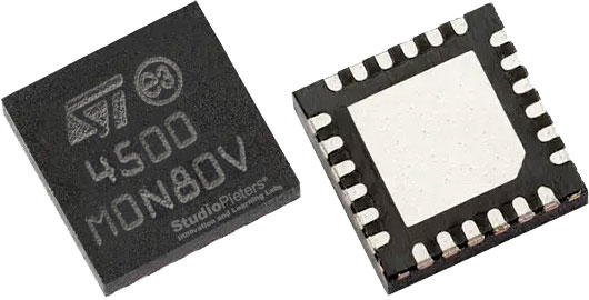
- STUSB4500: A standalone USB-PD IC by STMicroelectronics. This little chip is the brain that negotiates power delivery.
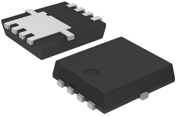
- STL6P3LLH6 MOSFET: The muscle that helps handle the power switching with style and grace.
With these two working together, I had the perfect duo for my design.

Enter KiCad: My Weapon of Choice
With my hardware sorted, it was time to whip out my favorite tool: KiCad. This open-source software has been my trusty sidekick for designing schematics and PCB’s. Armed with datasheets and a cup of coffee, I quickly drafted a schematic that combined the core components with a few supporting ones for good measure.

https://www.kicad.orgDownload KiCAD for free here!
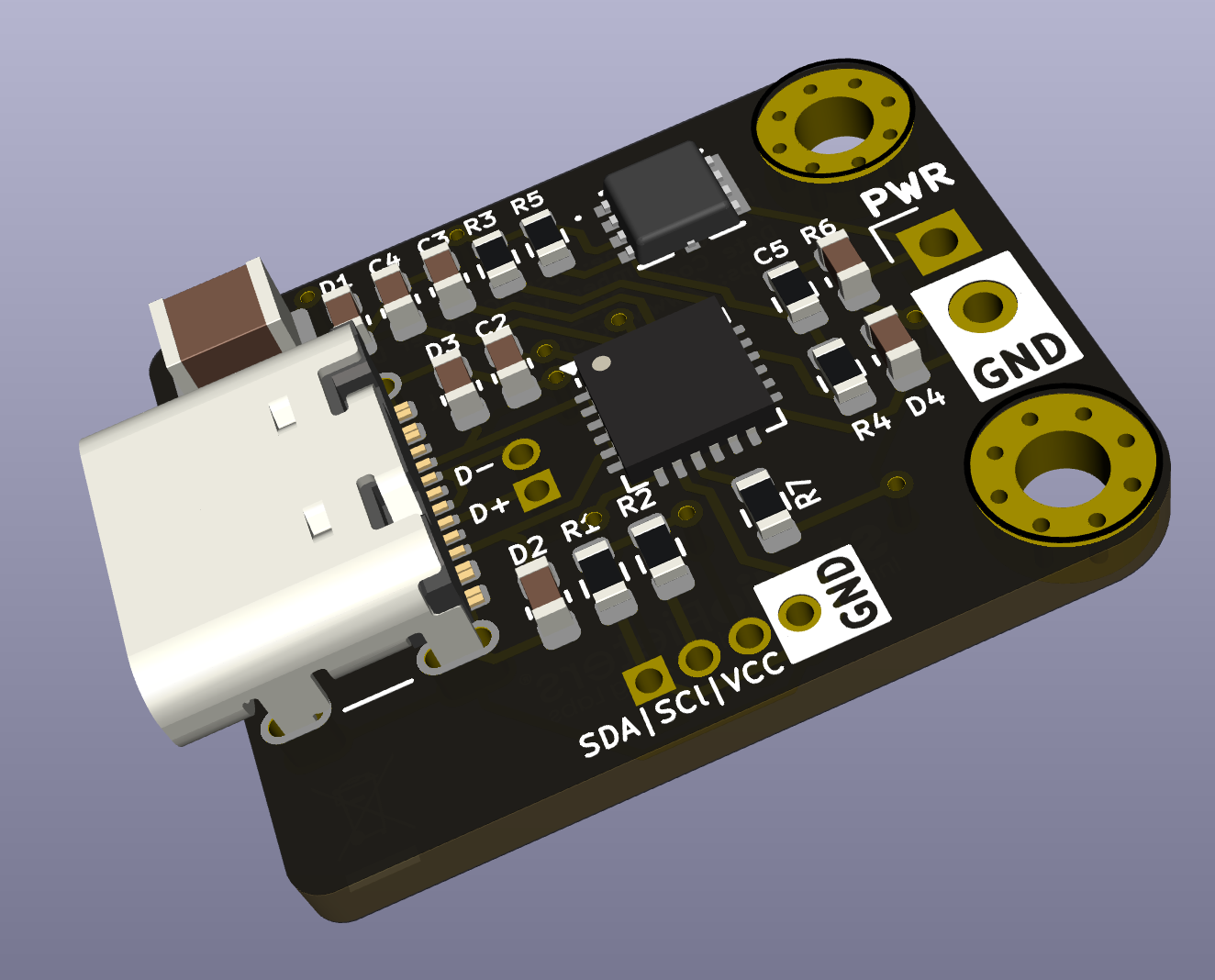
Breaking Down the Schematic
Let’s start at the USB port. It all begins with the CC1 and CC2 pins, which are responsible for communicating with the connected USB-C adapter to negotiate power levels. The STUSB4500 takes charge here, ensuring that the right voltage and current are delivered.
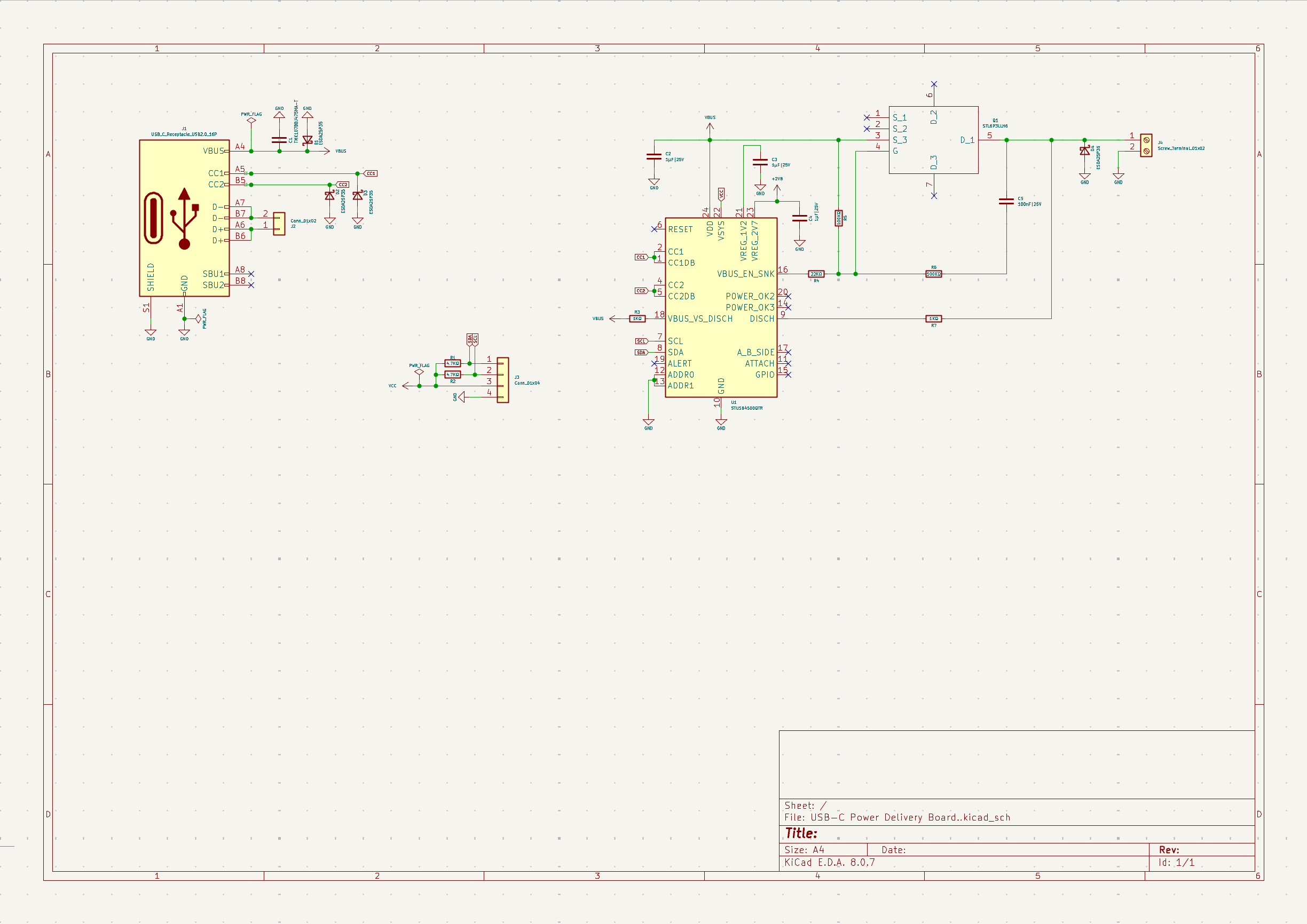
The STL6P3LLH6 MOSFET steps in to manage the high current gracefully, with a few resistors and capacitors sprinkled around to keep things stable. Add in some pull-up resistors, a bit of decoupling magic, and voilà! A schematic that’s both functional and elegant.
From Schematic to PCB: Let the Tetris Begin!
Designing a PCB is like playing Tetris—but with the stakes a little higher. My goal was to make the board as small as possible, while still including mounting holes for versatility. After a LOT of shuffling components around (and a few moments of “Nope, that trace won’t work!”), I ended up with a compact yet functional layout.
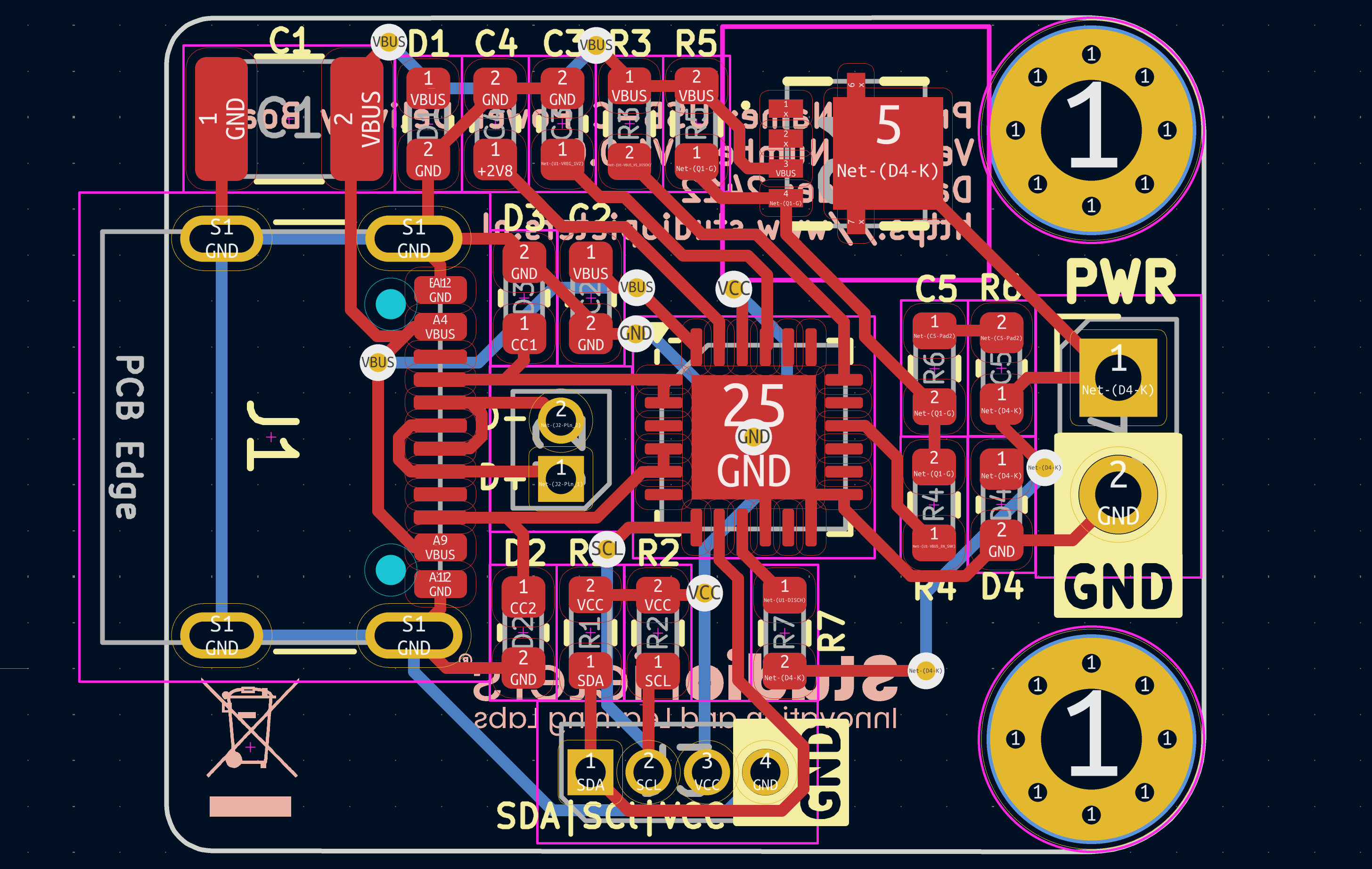
I kept a sharp eye on PCB design rules—no one wants a shorted connection or mismatched trace impedance ruining the party. The final design? Small, sleek, and ready for action.

Production Time: Hello, PCBWay!
With the PCB design complete and double-checked (because paranoia saves prototypes), it was time to hit send to my favorite manufacturer, PCBWay. Their consistent quality and reasonable pricing make them my go-to.
Use this link and get $5,00 of new user free credit!
Ordering Components: The Treasure Hunt
While waiting for the PCB’s to arrive, I turned my attention to sourcing components. I opted for Aliexpress for most parts—because where else can you buy 100 resistors and a mystery gift for $5? Of course, you could streamline this by letting PCBWay handleit all, but I like the hands-on experience of piecing everything together myself. Plus, there’s a strange satisfaction in unboxing tiny bags of components, knowing that they’ll soon come together to form something functional.
Assembly: Turning a Dream into Reality (Soon, Very Soon!)
When the PCB’s arrive, I imagine it’ll feel like Christmas morning—shiny, pristine boards fresh from PCBWay . I might just take a moment to admire them (let’s be honest, maybe even take a picture or two) before diving into assembly. Armed with my trusty soldering iron, some tweezers, and a magnifying glass, I’ll get to work placing components one by one.
Surface-mount soldering isn’t for the faint of heart, especially when dealing with tiny IC’s like the STUSB4500. But I’m ready for the challenge. I’ll keep my patience in check and, hopefully, my expletives to a minimum. There’s something immensely satisfying about seeing your design transform into reality, and I can’t wait to experience that.
What’s Next?
For now, it’s a waiting game. The PCB’s are on their way from PCBWay , and the components are slowly making their journey to me. In the next blog, I’ll share the unboxing, assembly, and testing process—hardware in hand, ready to shine.
Future iterations might include adjustable voltage output, additional protection circuitry, or even a tiny display for power monitoring. The possibilities are endless, and that’s the exciting part of DIY electronics.
Final Thoughts (For Now)
Designing this USB-C Power Delivery board has been a rewarding experience, even if the final steps are still on the horizon. It’s challenged me to think critically and creatively, and it’s given me a new appreciation for the art of hardware design. If you’ve ever wanted to create your own hardware, I encourage you to dive in. The journey is half the fun, and there’s something magical about seeing your design come to life—even if you have to wait a bit longer than expected.

Will you be here for the next blog? I hope so, because the best is yet to come. Until then, happy designing, and may your soldering iron always be hot (but not too hot). Stay tuned!